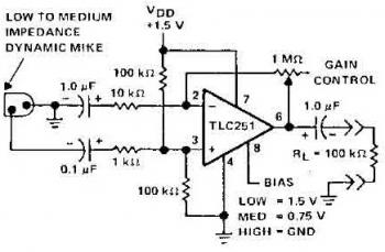
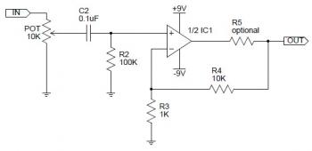
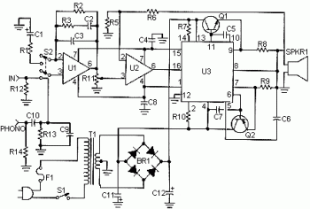
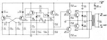
Here the schematic diagram of mic preamplifier which build based on operational amplifier TC251. The TLC251 is operating in low bias. The circuit works with only 1.5 V supply draws electric current of only 10 mA, so the battery operation will be prefered. Circuit frequency response is 3dB, 27 Hz to 4.8 kHz.
Home
Archives for 2011
Stereo Tube Power Amplifier Schematic
Tags
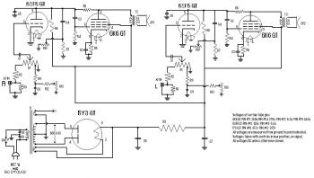
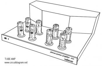
This is the circuit diagram of stereo tube power amplifier. It applies 3 types of tube that are 2 6SF5 GT high-mu triodes, 1 5Y3 GT vacuum rectifier, and 2 6K6 power beam amplifiers. The Audio input can be from any two-channel line level device such as a television, CD player, or VCR. It is of the tube type, using only 5 tubes total with no more than about 45 Watts power consumption from the outlet.
12 LED VU Meter Circuit
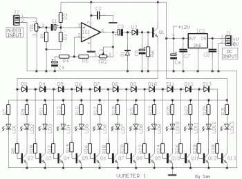
Here the 12 LED VU meter circuit. This is a simple visual indication of the audio level signals, adaptive to various user needs. Can be adapted to different input levels, adjustable by trimmer TR1 (state) - TR2 (Gain), then rectified by diodes D1-D2 (standard negative mark-recovery periods) and driven in the main circuit indication, consisting of the diodes D3 up to D13, transistors Q2-Q13 and materials that exist around them.
2-Way Active Crossover Circuit
Tags
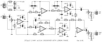
This is the schematic diagram of 2-way active crossover circuit. The "active" word means that the circuit use active component and need power supply to work. Take a note that the input of this circuit is not connected to the output of power amplifier. This crossover circuit module must be placed before the amplifier circuit. The "Low Out" output connected to a power amplifier and the low speaker [Woofer], while the "High Out" output is drive the power amplifier of high speaker [Tweeter].
Home Telephone FM Transmitter Circuit
Tags
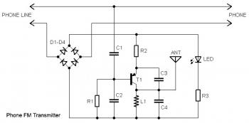
Here the schematic diagram of home telephone FM transmitter. This circuit connects in series with your home phone line and delivers the phone conversation through the FM band any time you pick up the telephone handset. Transmitted signal could be tuned by any FM receiver. The circuit features an "On Air" LED indicator and also gives you a switch that can be utilized to turn off the transmitter. A special characteristic of the circuit is the fact that no battery is required to operate the circuit because electrical power is taken from your phone line.
Stereo PLL FM Transmitter based BH1417
Tags
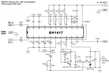
Here the circuit diagram of stereo PLL FM transmitter based BH1417 chip. This is certainly the most recent BH1417 FM Transmitter design diagram from RHOM that consists of lots of capabilities in a single tiny package. It includes pre-emphasis, limiter to ensure that the music can be transmitted at the same audio level, stereo encoder for stereo transmission, low pass filter that blocks any audio signals above 15KHz to avoid any RF interference, PLL circuit that delivers rock solid frequency transmission (no extra frequency drift), FM oscillator and RF output buffer.
FM Transmitter Circuit with MAX2606
Tags
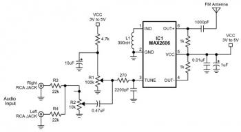
FM transmitter circuit which is build using single chip of MAX2606. A very simple FM transmitter connects your home-entertainment system to a portable radio that will be carried surrounding the house and into the back yard. As an example, it is possible to play music on the CD player in your private room, and listen to it on a portable radio by the back-yard barbeque.
80W Power Amplifier Circuit
Tags
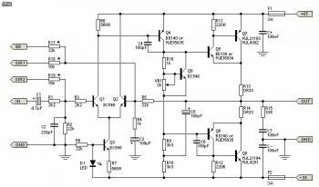
80W power amplifier circuit diagram based MJL4281A / MJL4302A and MJE15034 / MJE15035 power transistor. Actually the output power range is about 60W to 80W. This is an incredibly excellent amplifier. It's easy to construct, applies generally offered parts and is stable and well-performing. The diagram featured is really a full update on the original project, and even though it has a lot of similarities, is definitely a different design.
CMoy Headphone Amplifier Circuit
Tags
The following diagram is the circuit of CMoy headphone amplifier. Chu Moy designed a very popular headphone amplifier that’s easy to build, and it can be built small enough to fit in a pocket, power supply and all. It’s powerful enough to drive very inefficient headphones to thunderous volumes from even weak sources
CMoy headphone amplifier circuit diagram:
The op-amp used for this circuit is OPA2132PA, you may use OPA2132P or OPA2134PA as the alternative op-amp chip.
CMoy headphone amplifier circuit diagram:
The op-amp used for this circuit is OPA2132PA, you may use OPA2132P or OPA2134PA as the alternative op-amp chip.
Multi-color LED Driver Schematic
Tags
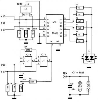
Have you ever wondered how many various colours can illuminate a LED? One, two or possibly three? Making this simple circuit, you will discover it a lot more. The important component in this design is a dual LED. One such accessory includes two inside the 'slices' of different diode LED, that each and every of them produces a different color (commonly green and red). For the drive needs three pins, a common cathode and two separate roots. In this way every single of the two integrated diodes can light up as independent of one another. You'll find only two colors that may create this dual LED.
6V Gel Cell Charger Circuit
Tags
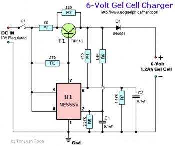
This is the diagram of 6V Gel Cell charger. The circuit is using NE555 timer as oscillator and TPI31T switching transistor. The schematic diagram designed by Tony Van Roon.
Parts List:
| R1 = 22 ohm, 1W
R2 = 270 ohm R3 = 220 ohm *R4 = 715 ohm, 1% *R5 = 3.57K, 1% *R6 = 1.40K, 1% *R7 = 1.47K, 1% | C1 = 100nF
C2 = 100nF D1 = 1N4001 T1 = TIP31A, B, C (or equivalent) U1 = Timer IC NE555V (or equivalent) S1 = Toggle switch, ON-OFF |
6V Gel Cell Charger circuit source page
6-8A / 0-28V Variable Power Supply Circuit
Tags
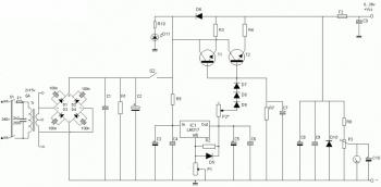
This is the schematic diagram of variable power supply. The output voltage of this power supply circuit can be adjust from 0V to 28V DC, while the current output is static the rang is about 6A up to 8A.
Parts List:
| R1 = 2K2 Ohm 2,5 Watt
R2 = 240 Ohm R3,R4 = 0.1 Ohm 10 Watt R7 = 6K8 Ohm R8 = 10K Ohm R9 = 47 Ohm 0.5 Watt R10 = 8K2 Ohm C1, C7, C9 = 47nF C2 = 4700uF/50v – 6800uF/50v C3, C5 = 10uF/50v C4, C6 = 100nF C8 = 330uF/50v C10 = 1uF/16v C11 = 22nF | D1…D4 = four MR750 diodes (MR750 = 6 Ampere diode) or 2 x 4 1N5401 diodes.
D5 = 1N4148, 1N4448, 1N4151 D6 = 1N4001 D10 = 1N5401 D11 = LED D7, D8, D9 = 1N4001 TR = 2 x 15 volt (30volt total) 6+- Ampere IC1 = LM317 T1, T2 = 2N3055 P1 = 5k P2 = 47 Ohm or 220 Ohm 1 Watt P3 = 10k trimmer pot F1 = 1 Amp F2 = 10 amp |
Source: circuitdiagram.net
Electronic Siren Circuit
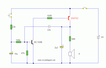
This is the schematic diagram of electronic siren circuit. The sound produced imitates the rise and fall of an American police siren. When very first switched on, the 10uF capacitors is discharged and each transistors are off. When the push button switch is pressed to 10uF capacitor will charge via the 22k resistor. This voltage is applied towards the base of the BC108B which will turn on slowly. When the switch is released the capacitor will discharge via the 100k and 47k base resistors and also the transistor will slowly turn off. The change in voltage alters the frequency of the electronic siren.
Electric current drain is fairly high in this electronic siren circuit so a appropriate power supply is needed. The duration the tone takes to rise and fall is determined by the 10uF and 22k resistor. These values may possibly be varied for various effects.
Simple LM358 Mic Preamplifier
Tags
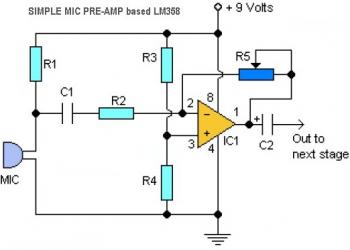
This is a simple LM358 microphone preamplifier schematic diagram. The pre-amp circuit is very easy to build and.. it's a low cost project... The variable resistor R5 is to adjust the LM358 op-amp gain. The LM358 has dual op-amp circuit modules, you may use a single LM358 to build two channels mic preamplifier.
Parts List:
R1, R3, R4 = 10K
R2 = 1K
R5 = 100K-1M Potensiometer
C1 = 0.1uF
C2 = 4.7uF/16V
IC1 = LM358 dual op-amp single power supply
Mic = Electret Microphone
Stereo FM Transmitter 88-108 MHz based BA1404
Tags
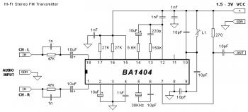
This is the stereo FM transmitter schematic diagram which built based BA1404. By using this HI-FI stereo FM transmitter, you will be able to transmit MP3 music from your iPod, computer, discman, walkman, TV / SAT receiver, and many other audio sources.
The transmitter can work from a single 1.5V cell battery and provide excellent crystal clear stereo sound. It can also be supplied from two 1.5V battery cells to provide the maximum range.
The kits of Stereo FM Transmitter 88-108 MHz based BA1404 available at electronics-diy.com, check it out
Offline Switching Power Supply Circuit (5V - 10A - 50W)
Tags
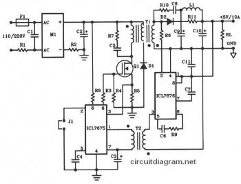
Here the schematic diagram of offline switching power supply:
Circuit Diagram:
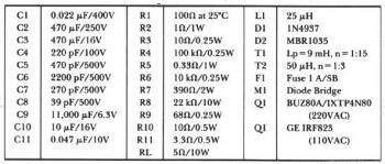
Parts List:
This switching power supply is using a MOSFET. For 220V AC voltage input, use BUZ80A/IXTP4N8 MOSFET and for 110V AC input voltage, use GE IRF823 MOSFET. The output will be 5 Volt DC with electric current can be reach 10A.
Circuit Diagram:
Parts List:
This switching power supply is using a MOSFET. For 220V AC voltage input, use BUZ80A/IXTP4N8 MOSFET and for 110V AC input voltage, use GE IRF823 MOSFET. The output will be 5 Volt DC with electric current can be reach 10A.
Echo Chamber Schematic
Tags
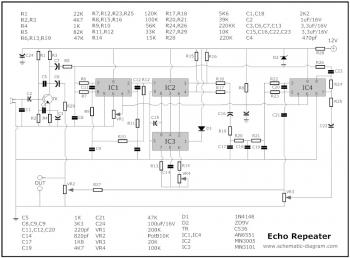
The following diagram is the schematic diagram of echo chamber circuit which will convert the sound of input to have echo sound like repeating sound if you talking in a cave. It will smoothing your sound also.
The circuit based 4 main ICs that are a MN3005, a MN3101, and 4 pieces of AN6551. I've made this kind of circuit, it's working great and you don't have to spend a lot of cost. :)
The circuit based 4 main ICs that are a MN3005, a MN3101, and 4 pieces of AN6551. I've made this kind of circuit, it's working great and you don't have to spend a lot of cost. :)
Clock Generator Circuit
Tags
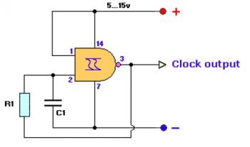
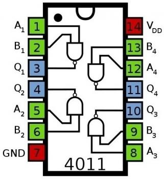
This is the circuit diagram of Clock Generator circuit based NAND logic gate. You can use 4011 for CMOS IC and 7400 for TTL IC.
Circuit Notes:
- Excellent clock generator to drive 4017 type CMOS circuits.
- Fo is ±1Kz when R1=100K and C1=10nF.
- R1 = 10K to 10M, C1 = 100pF to 47uF.
- Input voltage can be from 5 to 15V.
Sample IC CMOS NAND gate 4011 pinout:
Basic Motorcycle Alarm circuit
Tags
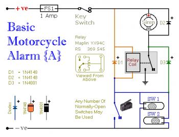
This is a very basic motorcycle alarm design circuit which can be used to secure your motorcycle with very low in cost.
Design schematic:
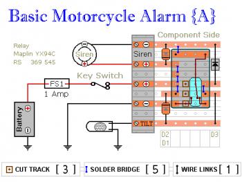
Circuit Number Five uses a SPCO/SPDT relay - but you actually only require to make use of a SPST relay. In case you are going to make use of the veroboard layout supplied - you will require to make use of the style of relay specified. But you are able to develop the alarm making use of whatever style of relay you've accessible.
Circuit Notes:
Any number of normally-open switches might be employed. Fit the mercury switches to ensure that they close when the steering is moved or when the bike is lifted off its side-stand or pushed forward off its centre-stand. Use micro-switches to secure removable panels and also the lids of panniers and so on. When 1 of the trigger-switches is closed - the relay will energize as well as the siren will sound.
You are able to select what will happen up coming. Should you develop the circuit as shown, the siren will continue to sound until you turn it off - or until the battery is exhausted. But, in the event you leave out D3 - the siren will stop sounding right away the trigger-switch is re-opened.
Whilst you are inside earshot of your machine - the former configuration is greatest. You are able to usually turn off the alarm your self. But in case you are going to be away from your bike for any length of time - and you do not wish to trigger a nuisance - then the latter configuration is possibly much more suitable. In the event you consist of a SPST switch in series with D3 - you'll be able to pick the behaviour that finest suits the circumstances at any given time.
Components placement:
Relay coils and some sounders generate high reverse-voltage spikes which will destroy sensitive electronic components. D1 and D2 are there to short-circuit these spikes just before they are able to do any harm. Even though there's absolutely nothing within the alarm circuit itself that might be damaged - I've no concept what other electronic equipment may be connected to the exact same power supply. So I included the two diodes as a precaution. If you are satisfied that there is absolutely nothing on your bike that may be damaged in this way - you'll be able to leave out the two diodes.
Basic Motorcycle Alarm circuit source: zen22142.zen.co.uk
Simple Servo Motor Controller circuit
Tags
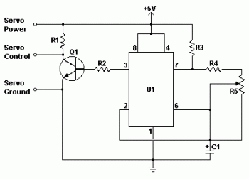
The following is the schematic diagram of simple servo motor controller circuit.
Simple Servo Motor Controller Parts List:
R1 = 820 Ohm 1/4W
R2 = 68K 1/4W
R3 = 10K 1/4W
R4 = 1K 1/4W
R5 = 1K Linear Taper Pot
C1 = 1uF/16V
Q1 = 2N3904 / 2N2222
U1 = 555 Timer IC
MISC = Board, Wire, Knob For R1, 8 Pin Socket For U1
The servo motor have many utilizes in everything from robotics to puppetry to photography and beyond. These tiny motors can position their output shaft to any position on command and hold that position. Most servos possess a range of motion to about 210 degrees and thankfully are quite easy to handle with a basic circuit like the one presented right here. Working with just a 555 timer as well as a couple of support parts, this circuit can handle a servo via it is full rotation primarily based on the position of a potentiometer.
Passive Surround Audio Circuit
Tags
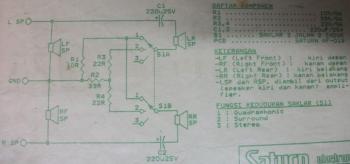
This is a passive surround audio circuit for better audio environment for your home audio system. The schematic diagram is very simple, it just need the combination of resistors and electrolytic capacitors.
Source: Passive audio surround
Passive Surround Audio Circuit Notes:
- The rear speakers must be full range type of speaker. Do not use woofer or tweeter speakers for rear speakers, you'll bad audio environment.
- 5W resistors is a must, the 1/4 or 1/2 watt resistor will burned.
Source: Passive audio surround
120V AC Line Powered LED
Tags
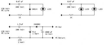
The following circuit diagram shows you about how to powering a LED (or two) from the 120 volt AC line applying | working with a capacitor to drop the voltage together with a little resistor to limit the inrush electric current. Considering that the capacitor need to pass current in both directions, a modest diode is connected in parallel using the LED to supply a path for the negative half cycle and also to limit the reverse voltage across the LED. A second LED using the polarity reversed could be subsituted for the diode, or perhaps a tri-color LED might be put to use which would appear orange with alternating current. The circuit is fairly efficient and draws only about a half watt from the line. The resistor value (1K / half watt) was chosen to limit the worst case inrush electric current to about 150 mA which will drop to much less than 30 mA in a millisecond as the capacitor charges. This appears to be a secure value, I've switched the circuit on and off several times without having harm to the LED. The 0.47 uF capacitor has a reactance of 5600 ohms at 60 cycles so the LED current is about 20 mA half wave, or 10 mA average. A bigger capacitor will boost the electric current along with a smaller 1 will lessen it. The capacitor should be a non-polarized kind having a voltage rating of 200 volts or a lot more.
The lower circuit is an demonstration of obtaining a low regulated voltage from the AC line. The zener diode serves as a regulator and also supplies a path for the negative half cycle electric current when it conducts inside the forward direction. In this example the output voltage is about 5 volts and will give over 30 milliamps with about 300 millivolts of ripple. Use caution when operating any electronic circuits hooked up straight to the AC line.
120V AC Line Powered LED circuit source:
http://www.bowdenshobbycircuits.info/page10.htm#lineled.gif
14W Audio Amplifier Circuit
Tags
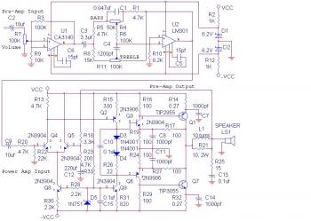
This Amplifier circuit designed by Mike Ellis at 1999. The amplifier capable to deliver up to 14W power audio output. The pre-amp circuit already designed in the circuit and direct connected to the amplifier modul.
Here the 14W Audio Amplifier schematic diagram:
For detailed explanation about this 14W amplifier circuit, visit the following page:
http://michaelgellis.tripod.com/audioamp.html
Here the 14W Audio Amplifier schematic diagram:
For detailed explanation about this 14W amplifier circuit, visit the following page:
http://michaelgellis.tripod.com/audioamp.html
Video Amplifier Circuit based LH0032
Tags
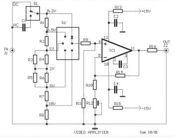
The following is the schematic diagram of Video Amplifier circuit, built based on LH0032, a high speed op-amp applications.
Video Amplifier Parts List:
R1 = 15Kohm+15Kohm
R2,R3,R4 = 10Kohm
R5,R6,R7,R8,R9 = 1Kohm
R10 = 820ohm
R11 = 1Mohm
R12 = 100ohm trimmer
R13,R15 = 47ohm
R14 = 10Kohm
C1 = 10uF 63V MKT
C2,C4 = 100nF 63V
C3 = 4.7pF ceramic
IC1 = LH0032
S1 = 1X2 mini switch
S2 = 1X6 sel.
J1,J2 = BNC connector
The LH0032 are very high speed general purpose operational amplifiers exhibiting 70 MHz bandwidths, 500 V/μs slew rates and 100 to 300 ns settling time to 0.1%. The LH0032 has the added advantage of FET input characteristics.
Fading LEDs Circuit
Tags
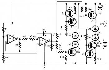
The following diagram is the schematic diagram of fading LEDs circuit. This kind of circuit runs two LED strips in pulsing mode, i.e. one LED strip goes from off state, lights up gradually, then dims little by little, and so on. while one other LED strip does the contrary.
Components part:
Circuit Works:

The IC1 contains two Op-Amps circuit which will be used to generate triangular wave form.. The rising and falling voltage obtained at pin #7 of IC1 drives two complementary circuits formed by a 10mA continual current source (Q1, Q2 and Q5, Q6) and driver transistor (Q3 and Q6).
R4, R5 & C1 are the timing components: the total period can be varied changing their values. R7 & R8 vary the LEDs brightness.
Fading LEDs Circuit Notes:
Fading LEDs Circuit Source: RedCircuits
Components part:
| R1, R2 = 4K7 R3 = 22K R4 = 1M * R5 = 2M2 * R6, R10, R11, R14, R15 = 10K R7, R8 = 47K Trimpot * R9, R13 = 27K R12, R16 = 56R | C1 = 1µF C2 = 100µF/25V D1-D4 etc = 5 or 3mm LEDs * IC1 = LM358 Q1, Q2 ,Q4 = BC327 Q3, Q5, Q6 = BC337 SW1 = SPST miniature Slider Switch B1 = 9V PP3 Battery |
Circuit Works:

The IC1 contains two Op-Amps circuit which will be used to generate triangular wave form.. The rising and falling voltage obtained at pin #7 of IC1 drives two complementary circuits formed by a 10mA continual current source (Q1, Q2 and Q5, Q6) and driver transistor (Q3 and Q6).
R4, R5 & C1 are the timing components: the total period can be varied changing their values. R7 & R8 vary the LEDs brightness.
Fading LEDs Circuit Notes:
- For those whishing to avoid the use of trimmers, suggested values for 9V supply are: R4=3M9, R9 & R13=47K and trimmers replaced by a short.
- Whishing to use a wall-plug adapter instead of a 9V battery, you can supply the circuit at 12V, allowing the use of up to 6 LEDs per strip, or at 15V, allowing the use of up to 7 LEDs per strip.
- In this case, the value of the trimmers R7 & R8 should be changed to 100K.
Fading LEDs Circuit Source: RedCircuits
50W Amplifier Circuit based ICL8063 + 2N3055
Tags
50W Amplifier Circuit, built based ICL8063 as power transsistor driver and 2N3055 as main power amplifier component.
50W Amplifier Circuit based ICL8063 + 2N3055 schematic diagram:
Parts List:
Circuit Notes:
50W Amplifier Circuit based ICL8063 + 2N3055 schematic diagram:
Parts List:
| R1 = 200 Ohm R2 = 200K R3 = 30K R5 = 1K R6 = 5K R7, R10 = 1 Meg R8,R9 = 0.4 Ohm/5Watt R11 = 10K Potensiometer R12,R13 = 51K R14 = 47K C1 = 100uF/35V C2 = 0.011uF C3 = 3750pF C4,C6 = 1000pF | C5,C7,C8 = 0.001uF C9 = 50pF C10 = 0.3uF C11,C12 = 10.000uF/50V U1,U2 = 741 Op Amp U3 = ICL8063 Audio Amp Transister Driver Q1 = 2N3055 NPN Power Transistor Q2 = 2N3791 PNP Power Transistor BR1 = 250 V 6 Amp Bridge Rectifier T1 = 50V Center Tapped 5 Amp Transformer S1 = SPST 3 Amp Switch S2 = DPDT Switch F1 = 2 Amp Fuse SPKR1 = 8 Ohm 50W Speaker |
Circuit Notes:
- Distortion is much less than 0.1% up to 100HZ and increases to about 1% at 20kHz.
- 50V CT transformer might be difficult to find, you may use 45V or 32V CT transformer.
- Q1 and Q2 should be use heatsinks to prevent over heating.
LM3886: 68W Power Amplifier
Tags
This is a good amplifier circuit taken from electronic-diy.com. Built based LM3886, the amplifier capable to deliver up to 68W audio output.
Parts List:
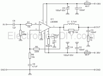
The amplifier should be supplied by +34 and –34 volts. R2 and L1 is a resistor of 10 ohms / 2 watt coiled with 10 to 12 you exhale of enameled thread AWG 20.
68W Power Amplifier circuit diagram based LM3886
Parts List:
| R1 = 10K Ohms R2 = 10 Ohms 2W see text R3 = 10 Ohms R4 = 47K Ohms R5 = 220K Ohms R6 = 10K Ohms R7 = 100K Ohms L1 0,7uH IC1 LM3886 | C1 = 100NF C2 = 100NF C3 = 100NF C4 = 100UF C5 = 100UF C6 = 4,7UF C7 = 100UF C8 = 1UF |
The amplifier should be supplied by +34 and –34 volts. R2 and L1 is a resistor of 10 ohms / 2 watt coiled with 10 to 12 you exhale of enameled thread AWG 20.
68W Power Amplifier circuit diagram based LM3886
25W Power Amplifier with MOSFET IRF530/IRF9530
Tags
This is a MOSFET powered amplifier circuit. The circuit output will be 25 Watt RMS @ 8 Ohm (1KHz sine wave) with frequency response of 30Hz to 20KHz -1dB.
Components Part:
Circuit Notes:
Components Part:
| R1, R4 = 47K R2 = 4K7 R3 = 1K5 R5 = 390R R6 = 470R R7 = 33K R8 = 150K R9 = 15K R10 = 27R R11 = 500R R12, R13, R16 = 10R R14, R15 = 220R R17 = 8R2 - 2W Resistor R18 = R22 - 4W Resistor (wirewound) | C1 = 470nF/63V C2 = 330pF/63V C3, C5 = 470µF/63V C4, C6, C8, C11 = 100nF/63V C7 = 100µF/25V C9 = 10pF/63V C10 = 1µF/63V Q1-Q5 = BC560C Q6 = BD140 Q7 = BD139 Q8 = IRF530 Q9 = IRF9530 |
Circuit Notes:
- This circuit dual polarity power supply to supply the amplifier.
- This audio amplifier can be directly connected to CD players, tuners and tape recorders. Just add a 10K Log potentiometer (dual gang for stereo) along with a switch to cope using the different sources you need.
- Q6 and Q7 must have a small U-shaped heatsink.
- Q8 and Q9 must be mounted on heatsink.
- Adjust R11 to set quiescent current at 100mA (best measured with an multimeter connected in series to Q8 Drain) with no input signal.
- A correct grounding is very important to eliminate hum and ground loops. Connect to the same point the ground sides of R1, R4, R9, C3 to C8. Connect C11 to output ground. Then connect separately the input and output grounds to power supply ground.
Electronic Chirping Canary Circuit
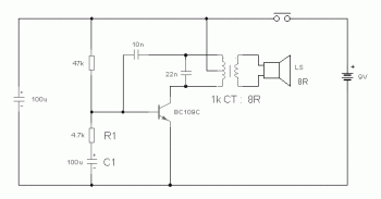
Well, for those of you who want to make a small project, this alarm may be an option for you. This circuit will generate the canary chirping sound. The chirp sound of a canary is generated by the oscillation process by resistor R1 and capacitor C1. The capacitor, having a capacitance value of 100 uF, is charging through the resistor, having a resistance of 4.7 K ohms. During this stage, R1 is the bias for the transistor making it operate in the cut off. When the transistor is in cut off mode, the base-emitter voltage is very minimal for any considerable current to flow. This mode triggers the oscillation to end but will start again once the capacitor discharges across the transmitter’s base-emitter circuit.
The frequency of the chirp may be modified by changing the values of the resistor and capacitor. The charging of the capacitor occurs when operating the push button switch. By releasing the button, the chirping runs quicker whilst the oscillation weakens.
The loudspeaker is being driven and coupled to the circuit by the miniature audio transformer of LT700 which having a frequency of 1 kHz. This circuit can be supplied with 9V battery.
Electronic chirping canary circuit source: http://www.elecpod.com/circuit/av/2010/03011410.html
100W Transistored Inverter 12VDC to 220VAC
Tags
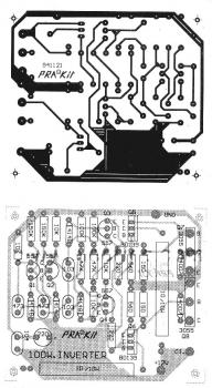
This inverter circuit can be used for medium electronic devices such as emergency light, radio, battery charger etc. Be carefull during assembly this circuit because of high voltage on the output transformer.
100W Inverter PCB Diagram:
100W Inverter PCB Design Layout:
Source of the circuit: 100W Interver Circuit
100W Inverter PCB Diagram:
100W Inverter PCB Design Layout:
Source of the circuit: 100W Interver Circuit
9V Mini FM Transmitter
Tags
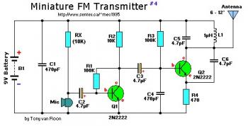
The following diagram is the circuit diagram of 9V Mini FM Transmitter.
Schematic diagram:
Components List:
R1,R3 = 100K
R2 = 10K
R4 = 470 ohm
C1,C4 = 470pF
C2,C3 = 4.7µF/16V
C5,C6 = 4.7pF
C7 = 4-40pF trimmer cap (optional, see text)
L1 = 1µH
Q1,Q2 = 2N2222, NPN transistor
Mic = Electret Microphone
B1 = 9 Volt battery
Circuit Notes:
Absolutely nothing crucial here. To get a bit of tuning out of the coil you could put a 4-40pF trimmer capacitor (optional) parallel over the 1 µH coil, L1.
C1/C4 and C5/C6 are ceramic capacitors, preferably NPO (low noise) types. C2/C3 are electrolytic or can be tantalum kinds.
In the event you determine to substitute transistors with some thing similar you already have, it perhaps necessary adjust the collector voltage of Q1 by changing the value of R2 or R3 (simply because you alter transistors, it changes this bias on the base of Q1). It ought to be about 1/2 the supply voltage (about four or 5v).
The antenna is nothing more than a piece of 12" wire or a piece of piano wire from 6" to 12".
To find the signal on your regular FM Radio dial, make certain there's a signal coming into the microphone, otherwise the circuit will not function. I use an old mechanical alarm clock (you know, with those two big bells on it). I put this clock by the microphone which picks up the loud tick-tock. I'm certain you get the concept... Or you can just lightly tap the microphone whilst looking for the location of the signal on your receiver.
The antenna is nothing more than a piece of 12" wire or a piece of piano wire from 6" to 12".
To find the signal on your standard FM Radio dial, make sure there is a signal coming into the microphone, otherwise the circuit won't work. I use an old mechanical alarm clock (you know, with those two large bells on it). I put this clock by the microphone which picks up the loud tick-tock. I'm sure you get the idea... Or you can just lightly tap the microphone while searching for the location of the signal on your receiver.
Source: http://www.sentex.ca/~mec1995/circ/fmt4.html
Design by Tony van Roon
Touch Activated Alarm
Tags
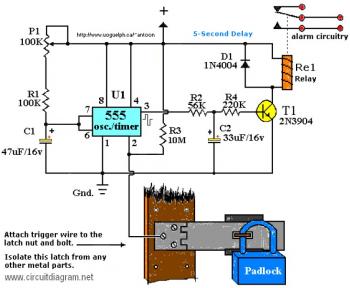
This is a touch activated alarm system. Your alarm system will be activated when someone touching the "trigger". You may use this circuit at your home door, your vehicle etc.
Parts list:
Notes:
*The 555 can be a LM, NE, or MC(cmos) type, they're all pin-compatible.
**C1/C2's working voltage ought to be elevated to 25V in the event you decide to go with a 12V power source. Rule of thumb: the operating voltage of capacitors are at least double the supplied voltage, in other words, if the power source is 9 Volt, your capacitor(s) is a minimum of 18V. Transistor T1 could be any approximate substitute.
*** Use any appropriate relay for the project and if you're not tight on area, use any size. I've build this specific circuit to prevent students from fiddling using the security cameras in pc labs at the University I'm employed. I made sure the metal casing was not grounded. But as being the schematic shows you are able to essentially hook it as much as any type of metal surface. I utilized a 12-vdc power supply. Use any suitable relay to deal with your specifications. A 'RESET' switch (Normally Closed) can be added between the constructive and also the 'arrow-with-the-+'. The trigger (touch) wire is connected to pin 2 of the 555 and will trigger the relay, using the body resistance, when touched. It is apparent that the 'touching' component has to be clean and can make good contact using the trigger wire. This particular circuit might not be suitable for all applications. Just in case you wonder why pin 5 is not listed within the schematic diagram; it is not really required. In particular noisy circumstances a little ceramic capacitor is placed between pin 5 and ground. It will no harm to put one or leave it out.
Additional note: For those of you who didn't discover, there's an approximate 5-second delay build-in before activation of the relay to avoid false triggering, or perhaps a 'would-be' thief, and so on.
Circuit design by Tony van Roon.
Parts list:
| R1 = 100K R2 = 56K R3 = 10M R4 = 220K P1 = 100K D1 = 1N4004 | T1 = 2N3904, or equivalent U1 = 555 Timer* C1 = 47μF/16V** C2 = 33μF/16V** Re1 = Relay*** |
Notes:
*The 555 can be a LM, NE, or MC(cmos) type, they're all pin-compatible.
**C1/C2's working voltage ought to be elevated to 25V in the event you decide to go with a 12V power source. Rule of thumb: the operating voltage of capacitors are at least double the supplied voltage, in other words, if the power source is 9 Volt, your capacitor(s) is a minimum of 18V. Transistor T1 could be any approximate substitute.
*** Use any appropriate relay for the project and if you're not tight on area, use any size. I've build this specific circuit to prevent students from fiddling using the security cameras in pc labs at the University I'm employed. I made sure the metal casing was not grounded. But as being the schematic shows you are able to essentially hook it as much as any type of metal surface. I utilized a 12-vdc power supply. Use any suitable relay to deal with your specifications. A 'RESET' switch (Normally Closed) can be added between the constructive and also the 'arrow-with-the-+'. The trigger (touch) wire is connected to pin 2 of the 555 and will trigger the relay, using the body resistance, when touched. It is apparent that the 'touching' component has to be clean and can make good contact using the trigger wire. This particular circuit might not be suitable for all applications. Just in case you wonder why pin 5 is not listed within the schematic diagram; it is not really required. In particular noisy circumstances a little ceramic capacitor is placed between pin 5 and ground. It will no harm to put one or leave it out.
Additional note: For those of you who didn't discover, there's an approximate 5-second delay build-in before activation of the relay to avoid false triggering, or perhaps a 'would-be' thief, and so on.
Circuit design by Tony van Roon.
Emergency Light and Alarm circuit
This is a simple and easy emergency light and alarm circuit. This circuit is permanently plugged into a mains socket and NI-CD batteries are trickle-charged. When a power outage occurs, the lamp automatically illuminates. Instead of illuminating a lamp, an alarm sounder can be chosen.
When power supply is restored, the lamp or the alarm is switched-off. A switch provides a "latch-up" function, in order to extend lamp or alarm operation even when power is restored.
Component parts list:
R1 = 220K
R2 = 470R
R3 = 390R
R4 = 1K5
R5 = 1R
R6 = 10K
R7 = 330K
R8 = 470R
R9 = 100R
C1 = 330nF/400V Polyester Capacitor
C2 = 10µF/63V Electrolytic Capacitor
C3 = 100nF/63V Polyester Capacitor
C4 = 10nF/63V Polyester Capacitor
D1-D5 = 1N4007
D6 = LED Green
D7 = 1N4148
Q1,Q3,Q4 = BC547
Q2,Q5 = BC327
SW1,SW2 = SPST Switches
SW3 = SPDT Switch
LP1 = 2.2V or 2.5V 250-300mA Torch Lamp Bulb
SPKR = 8 Ohm Loudspeaker
B1 = 2.5V Battery (two AA NI-CD rechargeable cells wired in series)
PL1 = Male Mains plug
Circuit Works:
Mains voltage is reduced to about 12V DC at C2's terminals, by means of the reactance of C1 and the diode bridge (D1-D4). This avoids the use of a mains transformer.
Trickle-charging current for the battery B1 is provided by the series resistor R3, D5 and the green LED D6 that also monitors the presence of mains supply and correct battery charging.
Q2 & Q3 form a self-latching pair that start operating when a power outage occurs. In this case, Q1 biasing becomes positive, so this transistor turns on the self latching pair.
If SW3 is set as shown in the circuit diagram, the lamp illuminates via SW2, which is normally closed; if set the other way, a square wave audio frequency generator formed by Q4, Q5 and related components is activated, driving the loudspeaker.
If SW1 is left open, when mains supply is restored the lamp or the alarm continue to operate. They can be disabled by opening the main on-off switch SW2.
If SW1 is closed, restoration of the mains power supply terminates lamp or alarm operation, by applying a positive bias to the Base of Q2.
Notes:
Emergency Light and Alarm circuit source: http://www.redcircuits.com/Page45.htm
When power supply is restored, the lamp or the alarm is switched-off. A switch provides a "latch-up" function, in order to extend lamp or alarm operation even when power is restored.
Component parts list:
R1 = 220K
R2 = 470R
R3 = 390R
R4 = 1K5
R5 = 1R
R6 = 10K
R7 = 330K
R8 = 470R
R9 = 100R
C1 = 330nF/400V Polyester Capacitor
C2 = 10µF/63V Electrolytic Capacitor
C3 = 100nF/63V Polyester Capacitor
C4 = 10nF/63V Polyester Capacitor
D1-D5 = 1N4007
D6 = LED Green
D7 = 1N4148
Q1,Q3,Q4 = BC547
Q2,Q5 = BC327
SW1,SW2 = SPST Switches
SW3 = SPDT Switch
LP1 = 2.2V or 2.5V 250-300mA Torch Lamp Bulb
SPKR = 8 Ohm Loudspeaker
B1 = 2.5V Battery (two AA NI-CD rechargeable cells wired in series)
PL1 = Male Mains plug
Circuit Works:
Mains voltage is reduced to about 12V DC at C2's terminals, by means of the reactance of C1 and the diode bridge (D1-D4). This avoids the use of a mains transformer.
Trickle-charging current for the battery B1 is provided by the series resistor R3, D5 and the green LED D6 that also monitors the presence of mains supply and correct battery charging.
Q2 & Q3 form a self-latching pair that start operating when a power outage occurs. In this case, Q1 biasing becomes positive, so this transistor turns on the self latching pair.
If SW3 is set as shown in the circuit diagram, the lamp illuminates via SW2, which is normally closed; if set the other way, a square wave audio frequency generator formed by Q4, Q5 and related components is activated, driving the loudspeaker.
If SW1 is left open, when mains supply is restored the lamp or the alarm continue to operate. They can be disabled by opening the main on-off switch SW2.
If SW1 is closed, restoration of the mains power supply terminates lamp or alarm operation, by applying a positive bias to the Base of Q2.
Notes:
- Close SW2 after the circuit is plugged.
- Warning! The circuit is connected to 230Vac mains, then some parts in the circuit board are subjected to lethal potential!. Avoid touching the circuit when plugged and enclose it in a plastic box.
Emergency Light and Alarm circuit source: http://www.redcircuits.com/Page45.htm
Amplifier Circuit based 4 Transistors
Tags
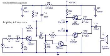
Above diagram very simple and easy to build class AB audio amplifier circuit which is working with 4 transistors. In class AB operation each output device performs more than half of the input signal cycle. Up to 78% effectiveness is possible with class AB designs and cross over distortion is minimized. The circuit shown here is appropriate for small radio receivers, audio players, intercom, phone etc.
Transistor Q1 with its connected parts is wired as a pre-amplifier stage. The audio input is coupled to the base of Q1 through resistor R1 and capacitor C1. Resistor R3 delivers collector to base bias for Q1 and C3 is an AC by pass capacitor for the collector resistor R4. Collector to base biasing is a great method of biasing for circuits like this because it provides enough negative feedback, prevents thermal runway and stabilizes the operating point. The second stage will be the driver stage for the push pull pair. Q2 with its connected parts carry out this job. This stage can also be collector to base biased, and its input is coupled towards the output from the pre-amplifier stage using capacitor C2. Resistor R8 limits the collector present of Q2.The third stage is the class AB push pull section comprising of transistors Q3 and Q4. Diodes D1 and D2 provides the bias voltage for the push pull stage. The output from the amplifier is coupled to the loud speaker through the capacitor C4. C5 and C6 are power supply filter capacitors.
Notes:
- The circuit can be assembled on a vero board.
- K1 may be an 8 ohm/5Wof loud speaker.
- C6 must be grounded near towards the Q1 and C5 should be grounded near to the loud speaker ground. This reduces noise.
- Use 5V DC power supply for powering the circuit.
EL34 Stereo Tube Amplifier 2x90 Watts
Tags
The following are step by step how to create a stereo tube amplifier using EL34 power tube. This stereo tube amplifier circuit is capable of producing an audio output of 90 watts for each channel.
Download EL34 Stereo Tube Amplifier 2x90 Watts step by step guide.
Download Link
Download EL34 Stereo Tube Amplifier 2x90 Watts step by step guide.
Download Link
220V Light Dimmer circuit
Tags
The following diagram is the schematic diagram of 220V Light Dimmer.
R1 = 10K
R2 = 2K2
R3 = 180K
Potentiometer 250K
C1 = 150nF/400V dipped polyester
C2 = 47nF/630V dipped polyester
C3 = 220nF/250V AC dipped polyester
Triac = 2N6075 or BT136-500D
Diac = HT-32
FUSE 2A or 3A
Download the 220V Light Dimmer circuit documentation here.
220V Light Dimmer diagram:
Parts List:R1 = 10K
R2 = 2K2
R3 = 180K
Potentiometer 250K
C1 = 150nF/400V dipped polyester
C2 = 47nF/630V dipped polyester
C3 = 220nF/250V AC dipped polyester
Triac = 2N6075 or BT136-500D
Diac = HT-32
FUSE 2A or 3A
Download the 220V Light Dimmer circuit documentation here.
35W Power Amplifier Circuit using STK082
Tags
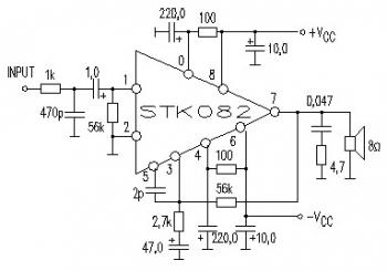
The following is the schematic diagram of 35W power audio amplifier. Built based on power-amp IC of STK082, this circuit will give great audio output for your home audio system.
Download the STK082 datasheet
Download the STK082 datasheet
Easy LED Flasher Schematic
Tags
Here the schematic diagram of Easy LED Flasher circuit:
Parts List:
This circuit will flash a bright or high-brightness red LED (5000+ mcd). Very good for fake car alarm or other attention getting device. Part values are not significant, test something else to start with from your junkbox.Certainly, the 470 ohm resistor (R3) determines the LED's brightness and limits the current supply to around 20mA. R3 value of 390 ohm may also be applied as a save value.
If you decide to go using a green or yellow led, which take more current, you might want to change the 470 ohm with an suitable value. Flash speed is established by R2 and C1 and is roughly three time constants (3*R2*C1). R1 provides bias to Q1 which ought to be small enough not to saturate Q2 with the capacitor disconnected. When the circuit doesn't oscillate, R1 may be very low or R2 too high. D1 allows for highter duty cycle operation and limits the feedback at the base of Q1 to -0.7 volts. D1 might be ommited for low supply power like 6 - 9V and low duy cycle operation.
Parts List:
| R1 = 10M ohm R2 = 1K – 100K ohm R3 = 470 ohm C1 = 0.47μF – 10μF/25V | D1 = 1N914 Q1 = 2N3904 Q2 = 2N3906 Led = High Brightness Red LED |
This circuit will flash a bright or high-brightness red LED (5000+ mcd). Very good for fake car alarm or other attention getting device. Part values are not significant, test something else to start with from your junkbox.Certainly, the 470 ohm resistor (R3) determines the LED's brightness and limits the current supply to around 20mA. R3 value of 390 ohm may also be applied as a save value.
If you decide to go using a green or yellow led, which take more current, you might want to change the 470 ohm with an suitable value. Flash speed is established by R2 and C1 and is roughly three time constants (3*R2*C1). R1 provides bias to Q1 which ought to be small enough not to saturate Q2 with the capacitor disconnected. When the circuit doesn't oscillate, R1 may be very low or R2 too high. D1 allows for highter duty cycle operation and limits the feedback at the base of Q1 to -0.7 volts. D1 might be ommited for low supply power like 6 - 9V and low duy cycle operation.
Easy Build RF Transmitter
Tags
This circuit most likely the easiest and simplest radio transmitter which you will get anyplace. It uses total of 5 components and could be built into a really compact space. It's very good for science fair projects or other science related projects in which a small range transmission is useful.
It works on 1.5 to 3 V, with small hearing aid battery packs or lithium "coin" cells becoming excellent. A thermistor or photoresistor may be inserted in series with R1 to get a various output frequency depending on the input.
The frequency may also be adjusted by modifying the value of C1. A 2N2222 transistor is highly recommended, but you are able to try out other types as well. Performance is likely to vary from type to type as well as from transistor to transistor. L1 is 20 to 30 turns of thin magnet wire (24 to 32 ga.) close wound about a 1/8 to 1/4" diameter non-conductive form. The coil is normally tapped 1/3 of the way from one end and also the tap connected to the emitter of Q1. Try out with all of the values in this particular circuit. Nothing is vital, but the result may be varied considerably.
Pipe Bomb Mic Construction
Tags
Pipe Bomb Mic Construction, by Jamie Heilman:
My own dimensions for my prototype are X= 36cm, Y= 5.5cm. This imparted a fairly high pitch tone but I like it.
The X and Y dimensions really should be played with to develop the precise tone your seeking, also I chose a telephone loudspeaker as well as a crystal mic so I got the funkiest tone I could think of. A dynamic microphone might limit the treble somewhat most likely make it sound less harsh. I’d be considering any mods produced to this style (ie. stories, suggestions, etc.) so feel free to e mail me.
The amps may be any old easy op-amp construction that can drive a loudspeaker or take a mic input. I just made use of some excess material I had lying around to make mine. The end product had all the circuitry inside the tube and the battery pack on the outside, with one control for the gain of the loudspeaker (mic was at fixed gain).
Note, in case you locate this in the front of the amplifier and turn every thing up, without having adding any dampening to the pipe, it will feedback just like you wont imagine! You'll most likely wish to keep away from this because it tends to hurt your ears. I put a bit of foam rubber in one end of the tube and an old sock in the other to dampen feedback. I like to leave my alternatives open though, so I also didn’t make this a permanent addition. My prototype is essentially a fuzz, as my guitar will overload the loudspeaker fairly simply and the pipe just adds a bit of strange overtone and what I believe is the smallest hint of reverb. Sounds excellent though! Clean tones via a similar set up would sound good too, but I haven’t constructed one of those yet. Possibly a larger speaker (4-5") and an old carpet pipe would probably add improved characteristics for clean tones. Attempt changing the tube material also for a various tone, I almost applied a bit of gutter piping when I 1st built this, right now I wonder what it would’ve sounded like.
Download the document about how to build Pipe Bomb Mic in PDF file:
Download Link
Transistored Stereo Tone Control
Tags
Here the circuit diagram of stereo tone control system which also available on the market in circuit kit, you might get the kit at electronic component/part store near your area. The tone control require 12v of supply voltage to work.
The circuit designed based on common tone control circuit, by using two transistors FCS9014 in each channel, so there are actually four transistors in this 12v stereo tone control. Take a note that you need to install the circuit prior to the amplifier device. The output of tone control should be connected towards the input of the audio amplifier. Any small signal NPN transistor such as BC547B, 2N3904, C828, or C945 may be put to use to replace FCS9014.
The circuit designed based on common tone control circuit, by using two transistors FCS9014 in each channel, so there are actually four transistors in this 12v stereo tone control. Take a note that you need to install the circuit prior to the amplifier device. The output of tone control should be connected towards the input of the audio amplifier. Any small signal NPN transistor such as BC547B, 2N3904, C828, or C945 may be put to use to replace FCS9014.
Very Easy R/C Circuit
Tags
The following diagram is a very easy and efficient receiver for actuating garage doors, starter motors, alarms, warning systems and numerous some other possibilities.
The SCR, that has a extremely low trigger present of 30 uA is common -- it requires an input electric power of just 30 uW to switch on the relay. A high Q tuned antenna circuit assures rejection of spurious signals. A whip or wire antenna is adequate as much as 100 feet from a low power transistor transmitter. A momentary-off switch resets the circuit.
The circuit specifies a whip or wire antenna which just indicates a solid piece of wire 6-12 inches long (15-30cm). The antenna coil is experimental, however you can start with ten to 12 turns of #22 (0.7mm) magnet wire, and 5/16" (8mm) coil diameter. Antenna wire is soldered at 1/2 turn of the coil and the gate of the BRY35 is soldered about halfway the coil. This circuit will transmit as much as 100-feet with the above specs @ 30uA.
The relay coil is specify's as much as 200 ohm but that's just the one I had in stock. Any low-ohm relay, even at 9V or so, ought to accomplish the task. And one remaining note, do not be expecting too a lot from this circuit. The "Very Easy R/C Circuit" is simply that; Easy!
The BRY35 is really an classic semiconductor produced by Philips. A great replacement would be the EC103D1, also produced by Philips (see pin-out picture for this device). NTE Semiconductors gives an alternative of NTE5405, but I have not attempted it. I think, a NTE5400 (30V) or NTE5401 (60V) will function just also. The NTE5405 is a bit overkill at 400V.
60W Inverter Circuit
Tags
Above circuit is a inexpensive completely transistorised inverter circuit ideal for driving medium loads of the order of 40 to 60 watts working with battery of 12V, 15 Ah or bigger power capacity.
Transistors T1 and T2 (BC548) make a 50Hz multivibrator. For having proper frequency, the values of resistors R3 and R4 may have to be modified after testing. The complementary outputs from Collectors of transistors T1 and T2 are provided to PNP darlington driver stages formed by transistor pairs T3-T4 and T6-T7 (utilising transistors BD140 and 2N6107). The outputs from the drivers are given to transistors T5 and T8 (2N3055) connected for push-pull operation.
Considerably bigger wattage could be achieved by growing the drive to 2N3055 transistors (by lowering the value of resistors R7 and R8 while increasing their wattage). Appropriate heatsinks may be applied for that output stage transistors to prevent the transistor from overheating. Transformer X1 is really a 230V primary to 9V-0-9V, 10A secondary used in reverse.
Download the document about this 12VDC to 230VAC 60W Inverter Circuit Here
Guitar Effect Circuit : Electro Harmonix Big Muff Pi
Tags
This Electro Harmonix Big Muff Pi circuit would most likely be better making the change by a contemporary input-jack power and a DPDT bypass switch. The kinds of transistors and diodes are unknown. It really is most likely that any high acquire NPN transistor and diode 1N914 will work. Coupling capacitors marked with * have been reported at its greatest if it has altered to 0.1uF and also the capacitors marked with ** modified to one.0UF. The unique transistors had been labeled SPT 87-103, and diodes of origin are marked or 525GY or 523GY (hard to examine.)
Download Electro Harmonix Big Muff Pi schematics in PDF:
Download Link
Subscribe to:
Posts (Atom)
