USB Battery Charger for Lithium Ion Battery

USB Battery Charger for Lithium Ion Battery circuit diagram

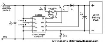
This schematic diagram is used for charging lithium ion battery. The power source is from a computer's USB port. With this circuit, you do not need to build power supply circuits for charging your battery.

A USB port is a great power source for charging a single cell li-on battery. It is capable of supplying maximum 5.25V and 500 mA. The circuit above is a USB powered single cell li-on battery charger. LM3622 is used as the controller. This special purpose IC has a precise end-of-charge control and low battery leakage current about 200nA.

Simple Battery Charger using LM350

Simple Battery Charger using LM350 circuit diagram

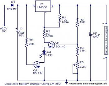
The schematic diagram can be used for charging the 12V lead acid batteries.

The circuit is designed as a constant voltage source with a negative temperature coefficient. The transistor Q1 (BD 140) is used as the temperature sensor. The transistor Q2 is used to prevent the battery from discharging through R1 when the mains power is not available. The circuit is designed based on the voltage regulator IC LM350. The output voltage of the charger can be adjusted between 13-15 V by varying the POT R6.

The LM350 will try to keep the voltage drop between its input pin and the output pin at a constant value of 1.25V. So there will be a constant current flow through the resistor R1. Q1 act here as a temperature sensor with the help of components R6/R3/R4 which more or less control the base current of Q1. As the emitter/base connection of transitor Q1, just like any other semiconductor, contains a temperature coefficient of -2mV/°C, the output voltage will also show a negative temperature coefficient. That one is only a factor of 4 larger, because of the variation of the emitter/basis of Q1 multiplied by the division factor of P1/R3/R4. This results in approximately -8mV/°C. The LED will glow whenever the mains power is available.

The transistor Q1 must be placed as close as possible to the battery.
Use a 20 to 30 V / 3A DC power supply for powering the circuit.
This circuit is not possible for charging GEL type batteries as it draw large amounts of current.

Here the LM350 pin layout:
 Here the LM350 pin layout

100 Watt Inverter 12V DC to 220V AC

Tags
Electronic schematic diagram for 100 Watt Inverter 12V DC to 220V AC.

100 Watt Inverter 12V DC to 220V AC circuit diagram

The IC1 Cd4047 wired as an astable multivibrator produces two 180 degree out of phase 1/50 Hz pulse trains.These pulse trains are are preamplifes by the two TIP122 transistors. The out puts of the TIP 122 transistors are amplified by four 2N 3055 transistors (two transistors for each half cycle) to drive the inverter transformer. The 220V AC will be available at the secondary of the transformer. Nothing complex just the elementary inverter principle and the circuit works great for small loads like a few bulbs or fans. If you need just a low cost inverter in the region of 100 W, then this is the best.

Notes:

  • A 12 V car battery can be used as the 12V source.
  • Use the POT R1 to set the output frequency to 50Hz.
  • For the transformer get a 12-0-12 V, 10A step down transformer. But here the 12-0-12 V winding will be the primary and 220V winding will be the secondary.
  • If you could not get a 10A rated transformer , don’t worry a 5A one will be just enough. But the allowed out put power will be reduced to 60W.
  • Use a 10 A fuse in series with the battery as shown in circuit.
  • Mount the IC on a IC holder.
  • Remember, this circuit is nothing when compared to advanced PWM inverters.This is a low cost circuit meant for low scale applications.

Design Tips:

The maximum allowed output power of an inverter depends on two factors. The maximum current rating of the transformer primary and the current rating of the driving transistors.

For example ,to get a 100 Watt output using 12 V car battery the primary current will be ~8A ,(100/12) because P=VxI. So the primary of transformer must be rated above 8A.

Also here ,each final driver transistors must be rated above 4A. Here two will be conducting parallel in each half cycle, so I=8/2 = 4A .

These are only rough calculations and enough for this circuit.

Bidirectional Power Inverter

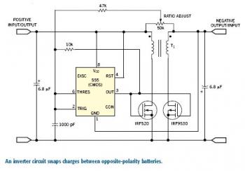
Bidirectional Power Inverter circuit diagram
Figure 1

If you want to swap charge in either direction between unevenly loaded positive and negative battery buses, you need an inverting dc transformer. One implementation is the symmetrical flyback converter shown in Figure 1. The circuit can generate a negative output from a positive supply or a positive output from a negative supply. When the circuit starts up, the substrate diode of the output FET bootstraps the output voltage to the point where synchronous switching takes over. When the gate-switching signal is symmetrical, the output voltage is approximately -95% of the input voltage, and the efficiency is greater than 80%. You can obtain voltage step-up or step-down by adjusting the switching ratio.

When I used the circuit between two 4V lead-acid batteries, a comparator adjusted the switch ratio to drive charge in the desired direction. The circuit automatically replaces charge drained from one battery to the other. In a short-battery-life application, the 2.5-mA standby current from each battery may be negligible. Using lower-gate-capacitance, FETs can reduce losses. Alternatively, you can add gates to the drive circuit to turn off both FETs whenever the battery voltages balance. The minimum input voltage is a function of the gate thresholds of the FETs. The ±9V rating of the CMOS 555 timer sets the maximum voltage. My prototype supplies approximately 100 mA.

source: www.edn.com

Inverter 12 V DC to 120 V AC

Tags
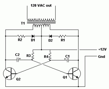
Inverter 12 V DC to 120 V AC circuit diagram

This Inverter takes 12 volt d.c and steps it up to 120 volt a.c. The wattage depends on which transistors you use for Q1 and Q2, as well as the "Amp Rating" of the transformer you use for T1. This inverter can be constructed to supply anywhere from 1 to 1000 (1 KW) watts. If Q1, Q2 are 2N3055 NPN Transistors and T1 is a 15 A transformer, then the inverter will supply about 300 watts. Larger transformers and more powerful transistors can be substituted for T1, Q1 and Q2 for more power.


Parts
C1, C2 >> 68 uf, 25 V Tantalum Capacitor
R1, R2 >> 10 Ohm, 5 Watt Resistor
R3, R4 >> 180 Ohm, 1 Watt Resistor
D1, D2 >> HEP 154 Silicon Diode
Q1, Q2 >> 2N3055 NPN Transistor (see "Notes")
T1 >> 24V, Center Tapped Transformer
Misc:
Wire, Case, Receptacle (for output)
Fuses, Heatsinks, etc.

Note: Don't try to run inductive loads (motors...) off this inverter.

Inverter 12V DC to 120-230V DC with IC 555

Tags
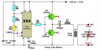
This DC-to-AC inverter schematic produces an AC output at line frequency and voltage. The 555 is configured as a low-frequency oscillator, tunable over the frequency range of 50 to 60 Hz by Frequency potentiometer R4.

Inverter 12V DC to 120-230V DC with IC 555 circuit diagram

Parts List:
R1 = 10K
R2 = 100K
R3 = 100 ohm
R4 = 50K potmeter, Linear
C1,C2 = 0.1uF
C3 = 0.01uF
C4 = 2700uF
Q1 = TIP41A, NPN, or equivalent
Q2 = TIP42A, PNP, or equivalent
L1 = 1uH
T1 = Filament transformer, your choice


The 555 feeds its output (amplified by Q1 and Q2) to the input of transformer T1, a reverse-connected filament transformer with the necessary step-up turns ratio. Capacitor C4 and coil L1 filter the input to T1, assuring that it is effectively a sine wave. Adjust the value of T1 to your voltage.

The output (in watts) is up to you by selecting different components.

Input voltage is anywhere from +5V to +15Volt DC, adjust the 2700uF cap's working voltage accordingly.

Replacement types for Q1 are: TIP41B, TIP41C, NTE196, ECG196, etc. Replacement types for Q2 are: TIP42B, TIP42C, NTE197, ECG197, etc. Don't be afraid to use another type of similar specs, it's only a transistor... ;-)
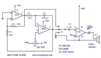
Multi tone alarm schematic diagram

electronic circuit diagram

This is a simple and easy to build multi tone alarm circuit that can be used in burglar alarms or sirens. The circuit is based on dual op-amp MC1458 and LM 380. The two op amps inside the MC 1458 are used to produce square and triangular waves.LM 380 is used to amplify the output.The first op amp IC1a is wired as an astable multi vibrator and second op amp IC1b is wired as an integrator, to make the square wave triangle.

The two output square ans sine can be selected using switch S1 to the input of IC2 which amplifies it to drive the speaker. POT R4 can be used for tone adjustment.

Notes .


www.circuitstoday.com

0 to 3V Adjustable Output Power Supply

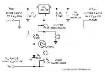
0 to 3V Adjustable Output  Power Supply circuit diagram

This is an LM317 based adjustable voltage regulator with a maximum output of 3V and 1.5A. The output voltage depends on the VIN, R1 and R2 values, so the circuit can be modified to use with a maximum output of greater than 3V. The maximum current output is also independent of the circuit design, it is related to the package options. In this circuit, LM317T, which is capable of transferring up to 1.5A, is used.

Since the internal reference voltage of the LM317 regulator is 1.25V, the output voltage can be also minimally 1.25V. One way to overcome this problem is using a reference voltage source built on two diodes. But this approach is mostly suitable for 1.5V to 15V regulators since the sensitivity becomes poor for the low voltage outputs less than 1.5 . On the other hand, diodes have temperature dependent forward voltages.

www.circuit-projects.com

General Purpose Power Supply

General purpose power supply schematics:
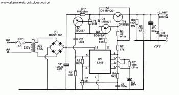
General Purpose Power Supply circuit diagram

You can select the output voltage range by 0-30V or 0-40V of 0-60V. The component's value will be different depends the output range you choose.

Vout Iout
R1
R4, R5 R9
Tr1
C1/C5
IC1
Tr2
Tr3
0-30V 1.3A
0.47Ohm
33k
2k7
24V/2A
40V
723
BD242
2N3035
0-40V 0.8A
0.82Ohm
47k
5k6
33V/1.5A
63V
L146
BD242A
2N3035
0-60V
0.6A
1.2Ohm
68k
19k
48V/1A
80V
L146
BD242B
2N3442


Please check the output current since higher voltage output will decrease the current output.