The following diagram is the schematic diagram of positive adjustable/variable power supply. It means that the power supply output will be DC current with positive [+] and ground [0] polarity.
Schematic diagram:
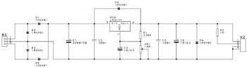
Power Supply Input:

Component part list:
R1 = 330
R2 = 1K
VR1 = 10K 10-turn trimpot
C1 = 2200uF/50V
C2,4 = 100nF ceramic
C3,4 = 10uF/63V
D1-6 = 1N5403
REG IC = LM317T
Heatsink
Visit this page to download the variable power supply diagram manual.
Schematic diagram:

Power Supply Input:

Component part list:
R1 = 330
R2 = 1K
VR1 = 10K 10-turn trimpot
C1 = 2200uF/50V
C2,4 = 100nF ceramic
C3,4 = 10uF/63V
D1-6 = 1N5403
REG IC = LM317T
Heatsink
Visit this page to download the variable power supply diagram manual.

