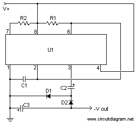
This simpe circuit will convert the positive input voltage become negative voltage.
Schematic diagram:
Component list:
| Part | Total Qty. | Description | |
| R1 | 1 | 24K 1/4 Watt Resistor | |
| R2 | 1 | 56K 1/4 Watt Resistor | |
| C1 | 1 | 3300pF 25V Ceramic Capacitor | |
| C2 | 1 | 47uF 25V Electrolytic Capacitor | |
| C3 | 1 | 10uF 25V Electrolytic Capacitor | |
| D1, D2 | 2 | 1N4148 Silicon Diode | |
| U1 | 1 | 555 Timer | |
| MISC | 1 | Wire, Board |
Notes:
- V+ can be anywhere from 4 to 16V. -V is one volt less than V+. So for -12V output, use +13V input. The maximum current output of the circuit is about 280mA, more than enough for a few op amps.
- For better regulation, a 79LOxx series regulator can be used.
- A zener diode may also be used to regulate the output voltage.

2 comments
ERRORS IN DESIGN:
1) PIN 4 needs ground
2) R1 and R2 are connected to pin 7 NOT to Vcc.
3) The values of R1 and R2 are switched
Please verify the schematic before post.
Alvaro,
pin 4 is a reset pin it connects to +vcc
R2 is between pins 6,2 to 7.not pin 8.
R1 and R2 values are reversed