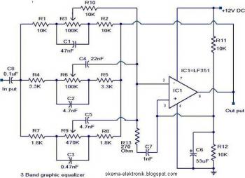
This schematic circuit diagram is very simple. Just need a single op amp IC LF351 (IC1) and few passive components.
The component values of this circuit are not very critical and can be replaced with nearest values with a little loss on the performance. This feature make it easy to be assembled from your junk box.
The op-amp LF351 is wired to operate in three frequency ranges- high,medium and low. The circuit is designed such that the circuit produces +/-20 dB boost or attenuation for 50Hz,1KHz and 10Khz by varying POT’s R3, R6 and R9. The maximum amplification for any of these bands at maximum supply voltage is 20dB. The op-amp LF 351 is wired as an inverting amplifier whose response to frequencies 50Hz,1Khz and 10KHz can be varied by adjusting POT’s R3,R6 and R9.
Notes:
- The circuit can be operated from 6 to 24 V DC .What I recommend is 12V .
- Use a 12V battery or 12 V DC power supply for the circuit.
- All capacitors must be rated 15V.
- A 10uF/15V capacitor must be connected between +ve and -ve pins of LF351 if the power supply is far from the circuit. Not shown in circuit.
